Three (and a half) ways to implement USB interface with an FPGA
Since its introduction almost 30 years ago, USB has developed into the most widely used interface to connect all sorts of electronic devices. Many microcontrollers provide USB interface on chip, but it is generally unavailable for small and low-cost FPGAs. Only relatively complex SoC-FPGA chips which include hard-core processor subsystem have USB inteface. However it is relatively easy to provide a USB connectivity using just an FPGA resources. Depending on a desirable connection speed (version of the USB interface) different implementation options are available.
Three (and a half) approaches to implement USB interface with an FPGA device are illustrated belo.
USB 1.1 (Low/High Speed, 1.5/12 Mbit/s)
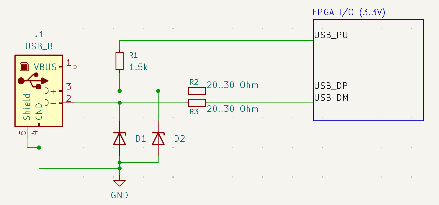
Most likely the smallest and simplest implementation of the USB 1.1 (1.5 or 12 Mbit/s) requires only 3 FPGA I/O pins (CMOS, 3.3V) and three resistors. Since there is no way to make it fully compliant with all the electical requirements of the specification and especially to survive through the specified failure scenarious, this implementation counts only as “a half”. However it is a working and easiest way to experiment with a USB interface. Even for a lab experiments a common mode chokes and ESD protection devices are strongly recommended.
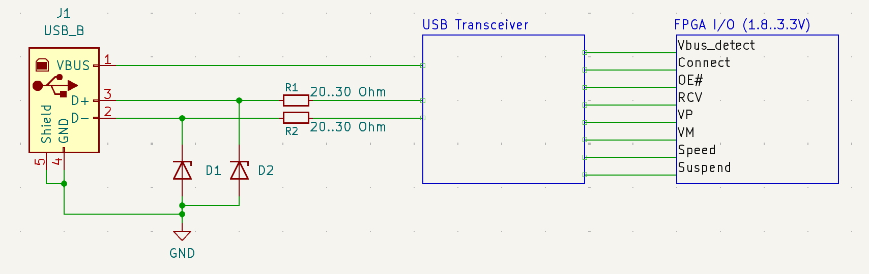
A specification compliant way to implement USB 1.1 interface with a FPGA GPIO signals is to use a dedicated USB driver/receiver chip. It would also allow to use low voltage (<3.3V) GPIOs, more widely available with modern FPGAs. This implementation also requires more than three IOs: four to eight, depending on desired additional functionality, such a low power (suspend) support, but that’s usually not a problem.
USB 2.0 (Full Speed, 480 Mbit/s)
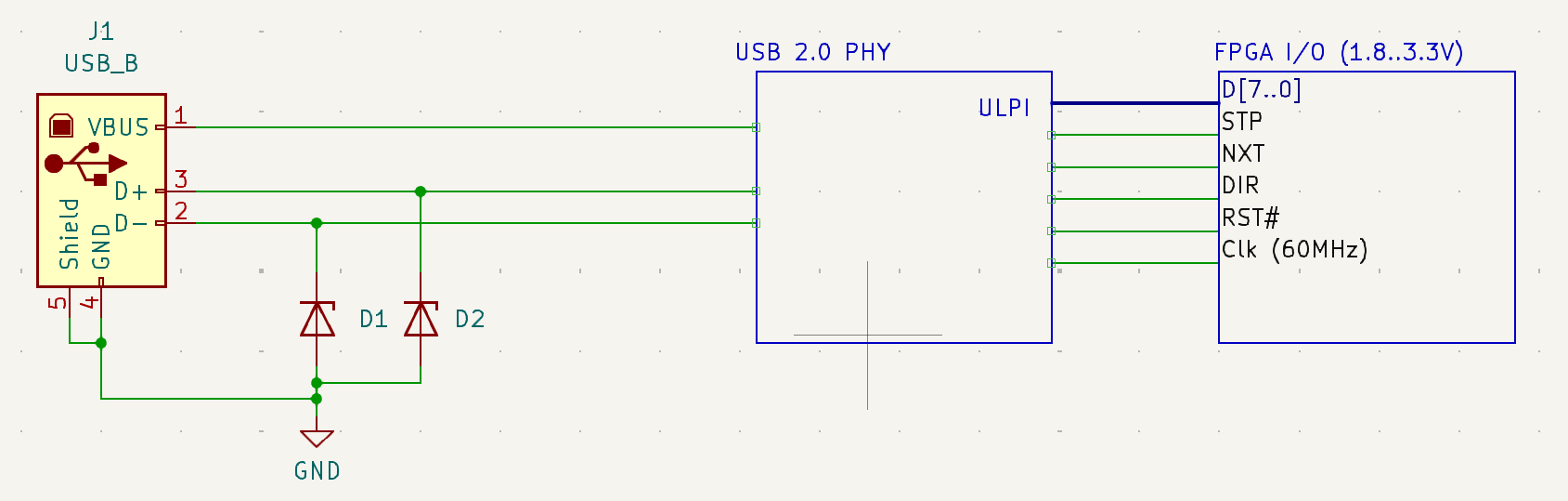
If a 12 Mbit/s maximum thoughtput of the USB 1.1 High Speed was not sufficient, a Full Speed introduced in USB 2.0 (480 Mbit/s) would be the next step. This mode (together with Low/High speed of USB 1.1) may be implemented by an external USB PHY device, connected to an FPGA via ULPI. The ULPI itself requires just 12 signals and a clock, but a sufficient care should be taken in both layout of a board and timing constraining of this interface in the FPGA design due to its relatively high frequency (60 MHz). Several USB PHYs with ULPI available from Microchip, Texas Instruments, and other vendors differes in their supported interface voltage, clocking schemes, and integrated additional features, such as line protection and switching, battery charging detection, etc.
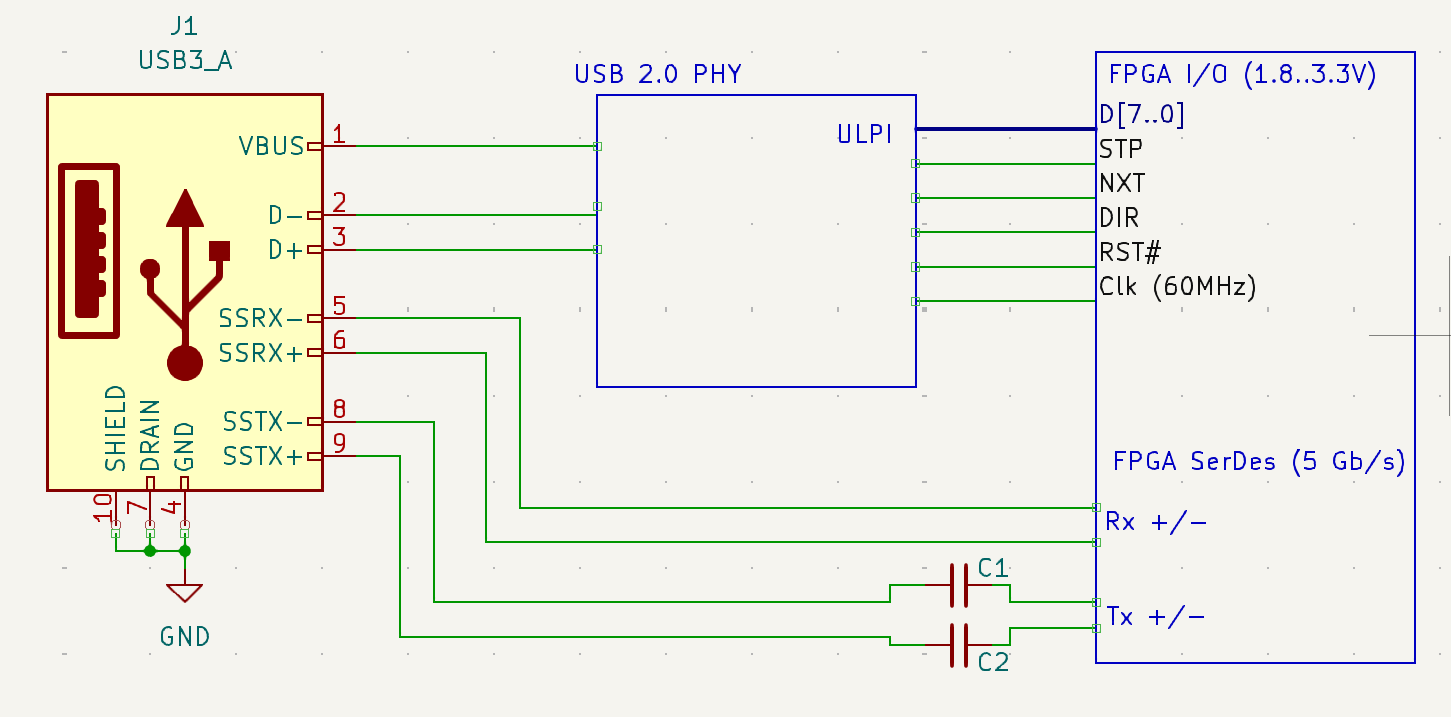
USB 3.2 Gen.1 (Super Speed, 5 Gbit/s)
A real challange starts with an implementation of more recent transceiver-based USB versions: it doesn’t only require a 5 Gbit/s (Super-Speed) or 10 Gbit/s (Super-Speed+) capable transceiver, with a support for LFPS (out-of-band signaling), but a separate suport for older USB interface for fallback mode if a transceiver link cannot be established for some reason. Reference clock generator, clock and data recovery circuitry, and PLL should met strict and diverse requirements for stability, jitter tolerance, and spread-spectrum clock support. At the same time high data throughtput require a wider data buses and pipelined processing inside an FPGA fabric and makes a design timing closure more difficult.