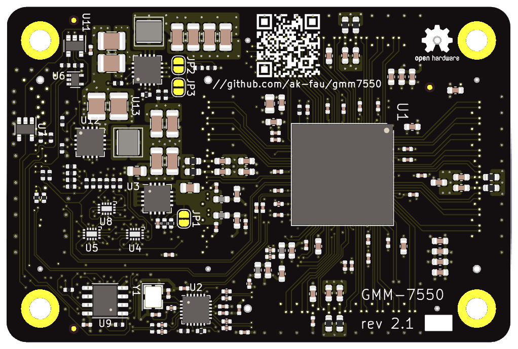
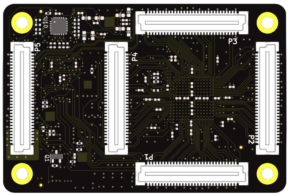
FPGA Module
| Top Side | Bottom Side |
|---|---|
 |  |
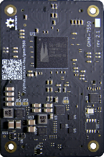 | 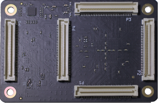 |
Cologne Chip GateMate FPGA
The module is based on the CCGM1A1 GateMate FPGA in BGA324 15x15 mm package. The FPGA provides:
- 20,480 programmable elements for combinatorial and sequential logic
- 20,480 8-input LUT-trees / 40,960 4-input LUT-trees
- 40,960 Latches / Flip-flops within programmable elements
- each programmable element configurable as:
- 1-bit full adder
- 2-bit full adder or
- 2x2-bit multiplier
- dedicated logic and routing for fast arithmetic and arbitrary-sized multipliers
- 9 general purpose input / output (GPIO) banks (8 available on the GMM-7550 module connectors)
- 162 user-configurable GPIOs (144 available on the module connectors)
- all GPIOs configurable as single-ended or LVDS differential pairs
- double data rate (DDR) registers in I/O cells
- I/O voltage range from 1.2 to 2.5 V
- 4 clock generators (PLL)
- maximum PLL output frequency from 250 MHz to 416.75 MHz
- 5 Gb/s serializer / deserializer (SerDes)
- flexible memory resources
- 1,310,720 total RAM bits distributed over 32 SRAM blocks
- each RAM block configurable as two independent 20 Kbit blocks or single 40 Kbit block
- simple or True Dual Port (SDP / TDP) or FIFO mode
- data width from 1 bit up to 40 bits (TDP) or 80 bits (SDP)
- bit-wide write enable
- error checking and correcting (ECC) for certain bit widths
- flexible device configuration
- application modes: low power, economy, speed (selectable with a solder jumpers on the module)
- 15x15 mm 324 balls 0.8 mm fine pitch Ball Grid Array (FBGA) package
Input Power and Converters
The module is powered from a single power supply in 2.9 to 6.5 V range, so it may be powered directly from a commodity 3.3 or 5 V power supply or a single Li-Pol cell.
On the module high-efficiency DC-DC converters generate the FPGA core supply voltage (hardware configurable to 0.9, 1.0, or 1.1 V), I/O voltage for the configuration interface, SPI-NOR FLASH, clock generator, and I/O banks (fixed at 2.5 V). The 2.5 V are provided on the module connectors to power a base board components.
Additional low-noise LDO regulator is provided for the FPGA high-speed serial transceiver and PLLs (hardware configurable 1.0 or 1.1 V).
The DC-DC convertes on the module are synchronized with the main module clock to reduce power supplies noise level. The converters operate at 1.25 MHz with a 180 degree phase shift to reduce inducted ripple on the input power feed.